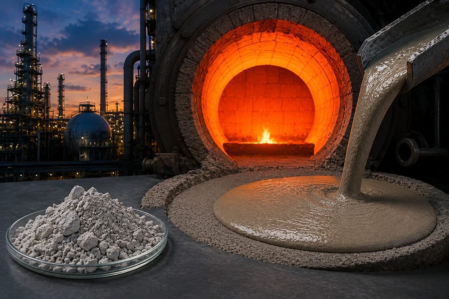
As wide bandgap semiconductors continue to drive innovation in power electronics and advanced crystal growth, 6N high purity α-form silicon carbide (SiC) has become a critical raw material. With a purity level of 99.9999%, this material is specifically engineered to meet the demanding requirements of third-generation semiconductor technologies and high-end crystal growth applications.
What Is 6N High Purity α-Form SiC?
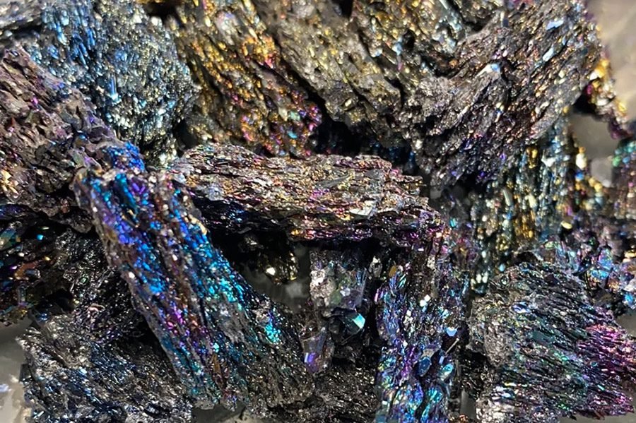
Silicon carbide (SiC) exists in multiple polytypes. Among them, α-SiC refers to the hexagonal crystal structures (such as 4H-SiC and 6H-SiC), which are thermodynamically stable at high temperatures and widely used for single-crystal growth.
6N high purity means the total impurity content is extremely low, typically measured in parts per million (ppm) or parts per billion (ppb). This ultra-high purity is essential because even trace impurities can significantly impact:
- Electrical conductivity
- Carrier concentration
- Crystal defect density
- Overall device performance
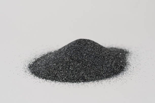
For this reason, 6N α-SiC powder is primarily used as a source material for Physical Vapor Transport (PVT) crystal growth.
Why High Purity Matters in SiC Crystal Growth
In SiC single-crystal growth, raw material quality directly determines the final wafer quality. High purity α-SiC offers:
- Stable sublimation behavior during PVT growth
- Lower unintentional doping, improving resistivity control
- Reduced crystal defects, such as micropipes and dislocations
- Higher yield and consistency in wafer production
This makes 6N α-SiC indispensable for both conductive and semi-insulating crystal growth.
N-Type 6N α-Form SiC
Definition and Characteristics
N-Type SiC contains carefully controlled amounts of donor impurities, most commonly nitrogen (N) or phosphorus (P). These elements introduce extra electrons into the crystal lattice, enabling electrical conductivity.
Key characteristics include:
- Controlled electron concentration
- Stable and predictable electrical behavior
- High compatibility with power semiconductor devices
Main Applications
N-Type 6N α-SiC is mainly used for:
- Growth of conductive SiC single crystals
- Substrate production for third-generation semiconductors
- Power devices, such as:
- MOSFETs
- Schottky barrier diodes (SBDs)
- High-voltage and high-frequency devices
Thanks to its wide bandgap, high thermal conductivity, and high breakdown field, N-Type SiC enables devices that operate at higher temperatures, voltages, and efficiencies than traditional silicon.
Semi-Insulating (SI) 6N α-Form SiC
Definition and Engineering Principle
Semi-Insulating SiC is engineered to block current flow. Unlike N-Type SiC, the goal here is not conductivity, but extremely high resistivity.
This is achieved by:
- Compensating donor and acceptor impurities
- Minimizing free carrier concentration
- Carefully controlling deep-level defects
The result is a material with resistivity typically greater than 10⁵–10⁹ Ω·cm.
Main Applications
Semi-Insulating 6N α-SiC is widely used for:
- Growth of semi-insulating SiC single crystals
- High-frequency and RF devices, such as:
- GaN-on-SiC RF substrates
- Microwave and millimeter-wave devices
-
Morganite crystal ingots and other specialty crystal growth applications
The high resistivity of SI-SiC minimizes parasitic conduction and signal loss, making it ideal for high-power and high-frequency electronics.
N-Type vs. Semi-Insulating SiC: Key Differences
| Aspect | N-Type SiC | Semi-Insulating SiC |
|---|---|---|
| Electrical behavior | Conductive | Highly resistive |
| Main dopants | Nitrogen, Phosphorus | Compensation-engineered |
| Free carriers | High electron concentration | Extremely low |
| Typical use | Power semiconductor substrates | RF, microwave, specialty crystals |
| Goal | Enable current flow | Block current flow |
https://www.silicon-carbides.com/blog/the-difference-between-n-type-and-semi-insulating-sic.html
Conclusion
6N high purity α-form SiC is a cornerstone material for advanced semiconductor and crystal growth industries. By tailoring impurity control and electrical properties, it can be supplied as either N-Type or Semi-Insulating, each serving distinct and critical roles.
- N-Type SiC supports the rapid growth of third-generation power semiconductors.
- Semi-Insulating SiC enables high-frequency, RF, and specialty crystal applications where ultra-high resistivity is essential.
As demand for high-performance electronics continues to grow, 6N high purity α-SiC will remain a key enabler of next-generation technologies.
Our Supply Capability
Henan Superior Abrasives can supply both N-Type and Semi-Insulating 6N high purity α-form SiC, specifically designed for advanced single crystal growth applications. With strict control over raw material purity, dopant levels, and batch consistency, our SiC materials meet the demanding requirements of conductive and semi-insulating SiC crystal growth.
We offer stable quality, customized electrical characteristics, and reliable supply to support customers in third-generation semiconductor, RF device, and specialty crystal manufacturing.