Для текстурирования задней поверхности пластин монокристаллического и мультикристаллического кремния требуется абразив, способный выполнять точную обработку., uniform micro-pit formation without introducing sub-surface lattice damage that degrades minority carrier lifetime. When the wrong abrasive is used — or when grit distribution is too broad — surface recombination velocity rises, pulling cell efficiency below the 22 % threshold that separates competitive PERC modules from commodity-grade output. For high-volume cell lines where a 0.3 % absolute efficiency loss across a 500 MW annual run translates directly to millions of dollars in lost energy yield, abrasive selection is not a secondary decision.
Why Green Silicon Carbide Is Preferred Over Black SiC for Solar Wafer Surfaces
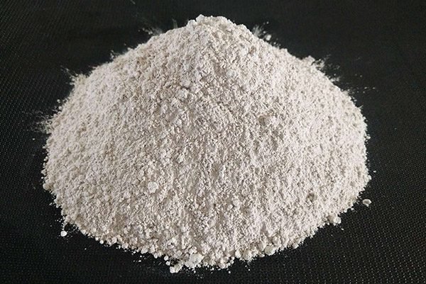
Both grades originate from the Acheson process, но зеленый карбид кремния (GSiC) is synthesized at higher furnace temperatures with lower metallic impurity loads — typically ≤ 0.05 % Fe and ≤ 0.03 % total heavy metals. On photovoltaic wafers, even trace iron contamination at the ppb level can form deep-level traps in the silicon bandgap, reducing diffusion length and increasing recombination. Черный карбид кремния, widely used in refractory and wear applications, carries higher residual impurity concentrations that are acceptable in thermal or structural contexts but incompatible with minority-carrier-sensitive surfaces. For a broader view of how silicon carbide manufacturing controls these variables, see Silicon Carbide Manufacturing Harnessing The Power Of This Versatile Material.
Green SiC also exhibits a tighter crystal morphology. Its blocky, sharp-edged particles fracture predictably under load, producing fresh cutting faces during lapping rather than rounding off and smearing. That self-sharpening behavior keeps material removal rates stable across a full wafer batch — a critical process-control advantage when back-surface roughness targets sit within a Ra ± 0.05 µm tolerance window.
Surface Texture Mechanisms: How GSiC Micro-Pits Reduce Optical Reflectance
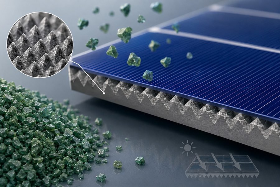
Effective back-surface texturing pursues two simultaneous optical objectives: scattering transmitted infrared light back into the absorber layer (light trapping) and reducing specular reflectance at the rear contact interface. Micro-pit density and geometry — not simply roughness amplitude — determine how well a textured surface achieves both. GSiC particles in the F600 to F1200 range (FEPA standard) create pit diameters of approximately 3–8 µm with aspect ratios sufficient to redirect photons at angles beyond the critical angle for total internal reflection in silicon (≈ 16.7°).
Lapping slurries formulated with GSiC at 20–35 % solids concentration, combined with a controlled pH between 9 а также 11, suppress particle agglomeration and maintain individual grain action. Agglomerates act as composite abrasive bodies that excavate trenches rather than discrete pits, producing anisotropic surface profiles that scatter light unevenly and reduce contact quality under aluminum BSF or PERC passivation stacks.
Grit Selection and Process Parameters: Matching Grade to Cell Architecture
Choosing the correct GSiC grit is a function of wafer thickness, target roughness, and the downstream passivation scheme. The following table summarizes recommended grades for three dominant back-surface architectures in current production:
| Cell Architecture | Recommended GSiC Grade (ПОДАЧА) | Target Ra (мкм) | Lapping Pressure (kPa) |
|---|---|---|---|
| Al-BSF (стандартный) | F600 – F800 | 0.25 – 0.40 | 18 – 25 |
| PERC (passivated emitter rear cell) | F800 – F1000 | 0.12 – 0.22 | 12 – 18 |
| TOPCon / SHJ rear side | F1000 – F1200 | 0.06 – 0.14 | 8 – 14 |
Finer grades used on TOPCon and silicon heterojunction architectures reduce the risk of micro-crack initiation in the ultra-thin (≤ 130 мкм) wafers common to n-type cell production. Sub-surface damage depth scales roughly with median particle diameter; GSiC F1200 limits damage depth to approximately 2–4 µm, well within the removal budget of subsequent KOH or HF-HNO₃ wet etching steps.
Slurry Management and Quality Control Checkpoints
Process consistency in back-surface texturing depends as much on slurry discipline as on initial grit selection. Распределение частиц по размерам (PSD) drift — coarsening caused by agglomeration or contamination — is the most common root cause of sudden Ra excursions in high-volume lines. Implementing the following controls reduces PSD-related rejects:
- Verify incoming GSiC lot PSD by laser diffraction (ИСО 13320) before releasing to production; reject any lot where D90 exceeds the specified upper bound by more than 8 %.
- Monitor slurry viscosity every 4 hours during operation; a viscosity rise above 15 % from baseline indicates water loss or contamination requiring slurry refresh.
- Filter recirculated slurry through 20 µm absolute-rated membrane filters to remove broken particle fragments and silicon swarf that accelerate tool wear and introduce scratch defects.
- Maintain slurry temperature at 22 ± 2 °С; elevated temperatures reduce suspension stability and accelerate silica gel formation on wafer surfaces.
- Replace slurry completely after each production campaign not exceeding 8 часы; cumulative particle rounding beyond that interval statistically correlates with Ra uniformity degradation exceeding 0.03 µm sigma.
Comparing GSiC with Alternative Abrasive Media for Photovoltaic Texturing
Diamond slurries, глинозем (Al₂O₃), and colloidal silica each compete with GSiC in specific segments of back-surface processing. Diamond delivers superior material removal rates and low sub-surface damage depth, but at 15–30× the per-liter cost of GSiC slurries, its use is typically confined to final polishing of high-efficiency concentrator cells rather than mass-production texturing. Alumina produces a more ductile removal mode that generates lower micro-crack density in some wafer orientations, but its lower hardness (Мооса 9 versus 9.2–9.5 for GSiC) results in faster media degradation and broader PSD drift over a production run.
Colloidal silica achieves sub-nanometer finish quality and is standard for chemical-mechanical planarization (CMP), but it is not suited to texturing — its removal mechanism is chemical rather than mechanical, producing surfaces that are too smooth (Ра < 0.01 мкм) for effective light scattering. GSiC occupies the performance-cost optimum for texturing applications that require controlled roughness, low contamination risk, and process repeatability at scale. Engineers familiar with Шлифовальные диски из карбида кремния will recognize similar reasoning behind choosing SiC over alumina for applications where a sharp, consistent cut geometry matters more than gentle stock removal.
Purity Specifications and Certification Requirements for Solar-Grade GSiC
Procurement teams sourcing GSiC for photovoltaic production should specify beyond basic grit sizing. Solar-grade material requires documented chemical analysis per IEC 60904 series quality frameworks and supply chain traceability to furnace batch level. Key purity thresholds that distinguish solar-grade from industrial-grade GSiC include SiC content ≥ 99.5 %, Fe ≤ 0.05 %, Al ≤ 0.10 %, and total heavy metals (Pb, Cd, Кр, Ni combined) ≤ 0.02 %. Suppliers should provide third-party XRF or ICP-OES certificates with each production lot, not just periodic product-level data sheets.
Magnetic susceptibility testing — often overlooked — identifies ferrous contamination that XRF may undercount in fine grit fractions. Requiring a maximum susceptibility of 0.05 × 10⁻⁶ m³/kg adds a practical incoming inspection step that correlates directly with in-process contamination risk. Unlike applications such as those explored in Black SiC In Refractory Materials, where bulk thermal performance dominates and trace metals are inconsequential, photovoltaic processing places strict electrochemical constraints on every material that contacts the wafer surface. Establishing these specifications contractually — not merely as guidance — protects cell efficiency targets and audit readiness under Tier-1 module qualification programs.
Часто задаваемые вопросы
Вопрос: What purity level of green silicon carbide is required for photovoltaic back-surface texturing?
А: Solar-grade green SiC should contain ≥ 99.5 % SiC by mass, with iron (Fe) ≤ 0.05 %, алюминий (Ал) ≤ 0.10 %, and combined heavy metals (Pb, Cd, Кр, Ni) ≤ 0.02 %. These thresholds prevent metallic contamination from forming deep-level recombination traps in the silicon bandgap, which can degrade minority carrier lifetime and reduce cell efficiency by 0.2–0.5 % absolute even at ppb contamination levels. Third-party ICP-OES or XRF certificates per production lot are standard practice among Tier-1 cell manufacturers.
Вопрос: Which FEPA grit grade should be used for texturing PERC cell back surfaces?
А: PERC back-surface texturing typically uses GSiC in the F800 to F1000 range, targeting a surface roughness Ra of 0.12–0.22 µm under lapping pressures of 12–18 kPa. Более грубые сорта (F600) risk exceeding the damage depth budget before KOH wet etching, while grades finer than F1000 may produce insufficient pit density for effective infrared light trapping in the 900–1100 nm wavelength range most relevant to PERC rear-side optical performance.
Вопрос: How does green SiC compare to black SiC for solar wafer applications?
А: Green SiC is synthesized at higher Acheson furnace temperatures, resulting in lower metallic impurity content (typically Fe ≤ 0.05 % vs. ≥ 0.1 % in black SiC) and a more ordered crystal structure. Black SiC performs well in refractory and structural wear applications where contamination tolerance is high, but its higher impurity load makes it unsuitable for wafer contact in photovoltaic processing. Green SiC also exhibits a tighter blocky particle morphology that maintains cutting sharpness longer per slurry refresh cycle.
Вопрос: How often should GSiC lapping slurry be replaced during continuous cell production?
А: Industry practice recommends complete slurry replacement after each production campaign not exceeding 8 continuous hours. Beyond this interval, cumulative particle rounding statistically correlates with Ra uniformity degradation exceeding 0.03 µm sigma, which triggers out-of-specification surface profiles for PERC and TOPCon architectures. Viscosity should also be monitored every 4 часы; a rise of more than 15 % above baseline indicates contamination or water loss requiring immediate slurry refresh rather than waiting for the scheduled replacement interval.
Вопрос: Can green silicon carbide slurry be used for front-side texturing of monocrystalline wafers as well?
А: Front-side texturing of monocrystalline silicon for standard cell architectures is predominantly performed using alkaline anisotropic etching (KOH or TMAH at 70–85 °C) to produce pyramidal structures aligned to the ⟨100⟩ crystal plane, which achieves reflectance below 2 %. Mechanical lapping with GSiC is not used for front-side mono texturing because it does not replicate the pyramid geometry that maximizes front-surface light coupling. GSiC slurry texturing is primarily applied to back surfaces and to multicrystalline wafers where crystal orientation randomness makes chemical pyramid etching ineffective.
О компании Henan Superior Abrasives (HSA)
Хэнань Улучшенные абразивы (HSA) является китайским производителем и глобальным поставщиком высокопроизводительных абразивных и современных керамических материалов для промышленного применения по всему миру.. Наш основной ассортимент продукции включает черный карбид кремния., зеленый карбид кремния, карбид кремния электронного класса (Карбид кремния), белый плавленый глинозем, коричневый плавленый глинозем, карбид бора, плавленые алюминаты кальция, и абразивы SG.
Обслуживание клиентов в 30+ страны, HSA поставляет надежные материалы для абразивов, огнеупоры, техническая керамика, полупроводниковые приложения, прецизионная полировка, пескоструйная обработка, металлургия, и высокоэффективные строительные материалы.
Получите предложение или бесплатный образец
Ищем надежного поставщика абразивных и современных керамических материалов премиум-класса.? Свяжитесь с нашей технической командой сегодня — мы ответим в течение 24 часов и можем организовать бесплатные образцы для квалифицированных проектов.
- 📧 Эл. адрес: sales@superior-abrasives.com
- 💬 WhatsApp: +86-186-3863-8803