

单晶硅片和多晶硅片的背面制绒需要能够精确研磨的磨料, 形成均匀的微凹坑,而不会引入会降低少数载流子寿命的次表面晶格损伤. 当使用错误的磨料时 - 或者当砂粒分布太宽时 - 表面复合速度会上升, 将电池效率拉至低于 22 % 区分竞争性 PERC 组件与商品级输出的门槛. 对于高容量细胞系,其中 0.3 % 绝对效率损失 500 兆瓦年运行直接导致数百万美元的能源产量损失, 磨料选择不是次要决定.
为什么太阳能晶圆表面首选绿色碳化硅而不是黑色碳化硅
两种牌号均源自艾奇逊工艺, 但 绿碳化硅 (硅碳化物) 在较高的炉温和较低的金属杂质含量下合成 - 通常 ≤ 0.05 % 铁和≤ 0.03 % 重金属总量. 在光伏晶圆上, 即使 ppb 级的微量铁污染也能在硅带隙中形成深能级陷阱, 减少扩散长度并增加复合. 黑碳化硅, 广泛应用于耐火和耐磨应用, 具有较高的残余杂质浓度,在热或结构环境中可以接受,但与少数载流子敏感表面不兼容. 更广泛地了解碳化硅制造如何控制这些变量, 看 利用这种多功能材料的力量进行碳化硅制造.
绿色碳化硅还表现出更紧密的晶体形态. 它是块状的, 锋利边缘的颗粒在负载下可预测破裂, 在研磨过程中产生新的切削面,而不是修整和涂抹. 这种自锐行为使整个晶圆批次的材料去除率保持稳定——当背面粗糙度目标位于 Ra ± 范围内时,这是一个关键的过程控制优势。 0.05 µm 公差窗口.
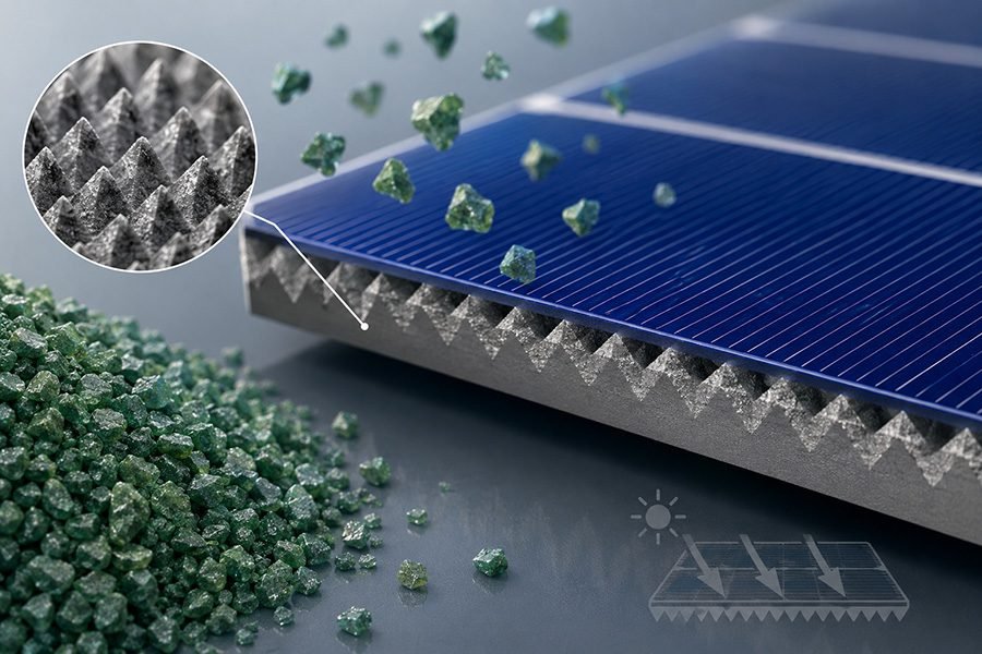
表面纹理机制: GSiC 微坑如何降低光学反射率
有效的背面纹理追求两个同时光学目标: 将透射的红外光散射回吸收层 (光捕获) 并降低后接触界面处的镜面反射率. 微坑密度和几何形状 — 不仅仅是粗糙度幅度 — 决定纹理表面实现这两者的效果. F600 至 F1200 范围内的 GSiC 颗粒 (FEPA标准) 创建约 3–8 µm 的凹坑直径,其纵横比足以以超出硅中全内反射的临界角的角度重定向光子 (约16.7°).
用 GSiC 在 20–35 配制的研磨浆料 % 固体浓度, 结合控制 pH 值 9 和 11, 抑制颗粒团聚并保持单个颗粒的作用. 团聚物充当复合磨料体,可挖掘沟槽而不是离散的凹坑, 产生各向异性表面轮廓,使光散射不均匀并降低铝 BSF 或 PERC 钝化叠层下的接触质量.
粒度选择和工艺参数: 将牌号与电池架构相匹配
选择正确的 GSiC 磨粒是晶圆厚度的函数, 目标粗糙度, 以及下游钝化方案. 下表总结了当前生产中三种主要背面架构的推荐牌号:
| 单元架构 | 推荐 GSiC 牌号 (喂养) | 目标Ra (微米) | 研磨压力 (千帕) |
|---|---|---|---|
| 铝基BSF (标准) | F600 – F800 | 0.25 – 0.40 | 18 – 25 |
| PERC (钝化发射极背面电池) | F800 – F1000 | 0.12 – 0.22 | 12 – 18 |
| 托普康 / SHJ后侧 | F1000 – F1200 | 0.06 – 0.14 | 8 – 14 |
TOPCon 和硅异质结架构上使用的更精细等级可降低超薄中微裂纹萌生的风险 (≤ 130 微米) n 型电池生产常用的晶圆. 次表面损伤深度大致与中值颗粒直径成正比; GSiC F1200 将损伤深度限制在大约 2–4 µm, 完全在后续 KOH 或 HF-HNO₃ 湿法蚀刻步骤的去除预算之内.
浆料管理和质量控制检查点
背面纹理化的工艺一致性不仅取决于初始砂粒选择,还取决于浆料规则. 粒度分布 (PSD) 漂移(由结块或污染引起的粗化)是大容量生产线中 Ra 突然偏移的最常见根本原因. 实施以下控制可减少与 PSD 相关的废品:
- 通过激光衍射验证传入的 GSiC 批次 PSD (国际标准化组织 13320) 在投入生产之前; 拒绝任何 D90 超过指定上限的批次 8 %.
- 每隔一段时间监测浆料粘度 4 运行期间的小时数; 粘度上升至以上 15 % 与基线相比表明失水或污染,需要更新浆料.
- 过滤再循环浆料 20 µm 绝对额定膜过滤器,可去除加速刀具磨损并引入划痕缺陷的破碎颗粒碎片和硅屑.
- 保持浆料温度在 22 ± 2 摄氏度; 高温会降低悬浮液稳定性并加速晶圆表面硅胶的形成.
- 每次生产后彻底更换浆料不超过 8 小时; 超过该区间的累积颗粒舍入与 Ra 均匀性退化超过统计相关 0.03 微米西格玛.
GSiC 与光伏纹理替代研磨介质的比较
金刚石浆料, 氧化铝 (铝2O₃), 和胶体二氧化硅在背面加工的特定领域与 GSiC 竞争. 金刚石具有卓越的材料去除率和低表面损伤深度, 但每升成本是 GSiC 浆料的 15-30 倍, 它的用途通常仅限于高效聚光电池的最终抛光,而不是大规模生产纹理化. 氧化铝产生更具延展性的去除模式,在某些晶圆方向上产生较低的微裂纹密度, 但其硬度较低 (莫氏 9 对比 GSiC 的 9.2–9.5) 在生产运行中导致更快的介质降解和更广泛的 PSD 漂移.
胶态二氧化硅可实现亚纳米级表面质量,是化学机械平坦化的标准 (化学机械抛光), 但它不适合纹理化——它的去除机制是化学的而不是机械的, 产生过于光滑的表面 (拉 < 0.01 微米) 用于有效的光散射. GSiC 对于需要控制粗糙度的纹理应用具有最佳的性能成本, 污染风险低, 以及大规模过程的可重复性. 熟悉的工程师 碳化硅砂轮 将认识到在尖锐的应用中选择 SiC 而不是氧化铝背后的类似原因, 一致的切削几何形状比温和的切削更重要.
太阳能级 GSiC 的纯度规格和认证要求
采购 GSiC 用于光伏生产的采购团队应指定基本粒度以外的内容. 太阳能级材料需要根据 IEC 进行化学分析记录 60904 系列质量框架和供应链可追溯至熔炉批次级别. 区分太阳能级和工业级 GSiC 的关键纯度阈值包括 SiC 含量 ≥ 99.5 %, 铁≤ 0.05 %, 铝≤ 0.10 %, 和总重金属 (铅, 光盘, 铬, 未合并) ≤ 0.02 %. 供应商应为每个生产批次提供第三方 XRF 或 ICP-OES 证书, 不仅仅是定期的产品级数据表.
磁化率测试 - 经常被忽视 - 识别 XRF 可能低估细砂粒部分中的含铁污染物. 要求最大敏感性 0.05 × 10⁻⁶ m³/kg 增加了实际的进货检验步骤,与过程中的污染风险直接相关. 与诸如中探索的应用程序不同 黑碳化硅在耐火材料中的应用, 其中体积热性能占主导地位,微量金属无关紧要, 光伏加工对接触晶圆表面的每种材料都施加了严格的电化学限制. 以合同方式制定这些规范(而不仅仅是作为指导)可以保护电池效率目标和一级组件资格计划下的审核准备情况.
经常问的问题
问: 光伏背面制绒需要什么纯度的绿碳化硅?
A: 太阳能级绿色SiC应含有≥ 99.5 % 碳化硅质量分数, 用铁 (铁) ≤ 0.05 %, 铝 (铝) ≤ 0.10 %, 和复合重金属 (铅, 光盘, 铬, 在) ≤ 0.02 %. 这些阈值可防止金属污染在硅带隙中形成深能级复合陷阱, 这会缩短少数载流子寿命并使电池效率降低 0.2–0.5 % 即使在 ppb 污染水平下也是绝对的. 每个生产批次的第三方 ICP-OES 或 XRF 证书是一级电池制造商的标准做法.
问: PERC 电池背面纹理应使用哪种 FEPA 粒度?
A: PERC 背面纹理通常使用 F800 至 F1000 范围内的 GSiC, 在 12–18 kPa 的研磨压力下,目标表面粗糙度 Ra 为 0.12–0.22 µm. 较粗的等级 (F600) KOH 湿法蚀刻前存在超出损伤深度预算的风险, 而比 F1000 更细的等级可能会产生不足的凹坑密度,无法有效捕获与 PERC 背面光学性能最相关的 900–1100 nm 波长范围内的红外光.
问: 在太阳能晶圆应用中,绿色 SiC 与黑色 SiC 相比如何?
A: 绿色碳化硅在较高的艾奇逊炉温度下合成, 从而降低金属杂质含量 (通常 Fe ≤ 0.05 % 与. ≥ 0.1 % 黑色碳化硅) 和更有序的晶体结构. 黑碳化硅在耐污染性较高的耐火材料和结构磨损应用中表现良好, 但其较高的杂质含量使其不适合光伏加工中的晶圆接触. 绿色碳化硅还表现出更紧密的块状颗粒形态,可以在每个浆料更新周期内保持更长的切割锋利度.
问: 连续电池生产过程中 GSiC 研磨浆应多久更换一次?
A: 行业实践建议每次生产活动后完全更换浆料,不超过 8 连续工作时间. 超出这个区间, 累积颗粒圆整与 Ra 均匀性退化超过统计相关 0.03 微米西格玛, 这会触发 PERC 和 TOPCon 架构的表面轮廓超出规格. 还应每隔一段时间监测粘度 4 小时; 涨幅超过 15 % 高于基线表示污染或失水,需要立即更新浆料,而不是等待预定的更换间隔.
问: 绿碳化硅浆料也可以用于单晶硅片的正面制绒吗?
A: 标准电池架构的单晶硅正面纹理化主要使用碱性各向异性蚀刻进行 (KOH 或 TMAH,70–85 °C) 产生与 ⟨100⟩ 晶面对齐的金字塔结构, 其反射率低于 2 %. 使用 GSiC 进行机械研磨不用于正面单纹理,因为它不复制最大化前表面光耦合的金字塔几何形状. GSiC 浆料制绒主要应用于背面和多晶硅片,其中晶体取向的随机性使得化学金字塔蚀刻无效.
关于河南高级磨料磨具 (高铁)
河南优之源磨料 (高铁) 是一家总部位于中国的制造商和全球供应商,为全球工业应用提供高性能磨料和先进陶瓷材料. 我们的核心产品系列包括黑碳化硅, 绿碳化硅, 电子级碳化硅 (碳化硅), 白刚玉, 棕刚玉, 碳化硼, 电熔铝酸钙, 和 SG 磨料.
服务客户于 30+ 国家, HSA 提供可靠的磨料材料, 耐火材料, 技术陶瓷, 半导体应用, 精密抛光, 喷砂, 冶金, 和高性能建筑材料.
获取报价或免费样品
寻找优质磨料和先进陶瓷材料的可靠供应商? 立即联系我们的技术团队——我们会在 24 小时并可为合格的项目安排免费样品.
- 📧 电子邮件: sales@superior-abrasives.com
- 💬 WhatsApp的: +86-186-3863-8803


