Полупроводниковые материалы из карбида кремния
Третье поколение полупроводников обладает превосходными характеристиками и более широкими возможностями применения.. Как основа развития электронных информационных технологий, полупроводниковые материалы претерпели несколько поколений изменений.. С более высокими требованиями сценариев применения, полупроводниковые материалы третьего поколения, представлен карбидом кремния и нитридом галлия, постепенно вступили в фазу индустриализации и ускоренного выпуска. По сравнению с предыдущими двумя поколениями, карбид кремния обладает превосходными характеристиками, такими как сопротивление высокому напряжению, высокая термостойкость и низкие потери, и широко используется для изготовления высокотемпературных, высокая частота, мощные и радиационно стойкие электронные устройства.
Карбид кремния устройства имеют широкий спектр применения. Из-за высокой теплопроводности, высокая напряженность электрического поля пробоя и высокая плотность тока, полупроводниковые устройства на основе материалов карбида кремния могут использоваться во многих областях промышленности, таких как автомобили, зарядные устройства, портативные источники питания, устройства связи, роботизированное оружие, и летательные аппараты. Сфера его применения становится все популярнее и углубляется., очень широкий спектр перспектив применения, очень ценные материалы.
Анализ преимуществ карбида кремния
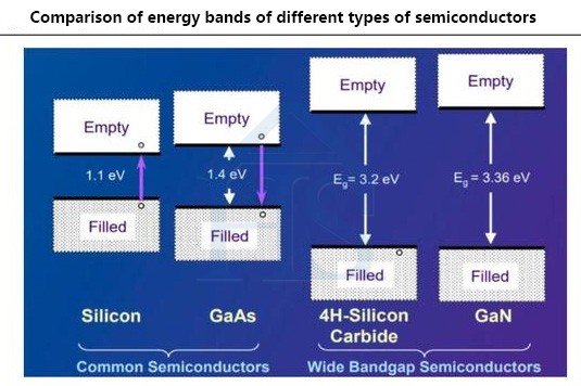
Ширина запрещенной зоны полупроводникового материала третьего поколения намного больше, чем у первых двух поколений.. Полупроводники первого и второго поколений представляют собой полупроводники с узкой запрещенной зоной., а от третьего поколения полупроводников, широкая полоса (ширина запрещенной зоны больше 2,2 эВ) полупроводниковые материалы стали использоваться в больших количествах. Карбид кремния, как типичный представитель полупроводников третьего поколения, имеет более 200 пространственные структуры, и разные структуры соответствуют разным значениям ширины запрещенной зоны, обычно между 2,4 эВ и 3,35 эВ. В дополнение к широкой полосе, материалы из карбида кремния также обладают преимуществами высокой напряженности поля пробоя., высокая скорость дрейфа насыщения и высокая стабильность, и максимальная мощность.
Широкая полоса: улучшить стабильность материала и напряженность поля пробоя
Ширина запрещенной зоны определяет свойства материала, широкая запрещенная зона для улучшения производительности. Широкая полоса пропускания является важным показателем производительности полупроводников.. Более широкая полоса означает более высокие требования к возбуждению, т.е., более сложное образование электронов и дырок, что приводит к широкозонным полупроводникам, которые сохраняют свойства изолятора, когда от них не требуется работать., что также делает их более стабильными, и широкая полоса также помогает улучшить напряженность электрического поля пробоя, что, в свою очередь, повышает способность противостоять рабочей среде, что отражено в лучшей термостойкости и стойкости к высокому напряжению, радиационная стойкость.
Большая разница энергий между зоной проводимости и валентной зоной в широкозонной системе снижает скорость соединения электронов и дырок после возбуждения., что позволяет использовать больше электронов и дырок для проводимости или теплопередачи, что является одной из причин более сильной тепло- и электропроводности карбида кремния..
На основании этих характеристик, устройства из карбида кремния могут работать с более высокой интенсивностью, а также способны быстрее рассеивать тепло, с более высокими предельными рабочими температурами. Характеристики стойкости к высоким температурам могут привести к значительному увеличению удельной мощности при одновременном снижении требований к системам отвода тепла., позволяет использовать более легкие и меньшие терминалы. Высокая ширина запрещенной зоны карбида кремния также позволяет устройствам из карбида кремния пропускать значительно меньший ток, чем кремниевые устройства., тем самым снижая потери мощности; устройства из карбида кремния не имеют остаточного тока в процессе отключения, что приводит к низким потерям переключения и значительному увеличению частоты переключения практических приложений.
Высокое напряжение пробоя: Обеспечение большего рабочего диапазона и диапазона мощности
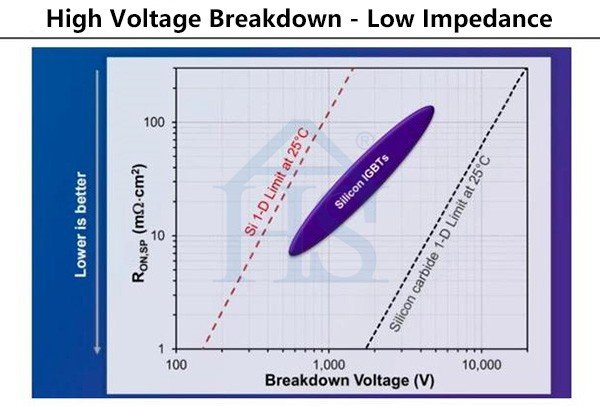
Чем выше напряжение пробоя, чем больше рабочий диапазон и диапазон мощности. Напряжение пробоя относится к напряжению, при котором происходит пробой диэлектрика.. Для полупроводников, после достижения напряжения пробоя, полупроводник теряет свои диэлектрические свойства и становится неработоспособным из-за разрушения своей внутренней структуры, что похоже на проводник. Следовательно, более высокое поле пробоя означает больший рабочий диапазон и диапазон мощности, т.е., тем выше поле пробоя, тем лучше.
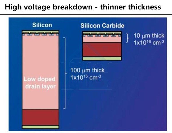
Устройства из карбида кремния более мощные., меньше, и имеют меньшие потери энергии. Из-за более высокого напряжения пробоя, карбид кремния может найти широкое применение при изготовлении мощных приборов, преимущество, которое нельзя заменить полупроводниками на основе кремния. Более высокий уровень разрушения карбида кремния позволяет силовым устройствам из карбида кремния иметь более тонкие и сильно легированные барьерные слои., что позволяет использовать карбидокремниевые материалы, чтобы сделать устройства тоньше при тех же требованиях, что может служить для экономии места и увеличения удельной плотности энергии. Кроме того, высокое поле пробоя также позволяет карбиду кремния иметь более низкое сопротивление в открытом состоянии при внешнем напряжении., а более низкое сопротивление во включенном состоянии означает меньшие потери энергии.
Высокая скорость дрейфа насыщения: меньше потерь энергии
Карбид кремния имеет более высокую скорость дрейфа насыщения из-за своей внутренней структуры.. Теоретически, скорость дрейфа может неограниченно возрастать с увеличением внешнего электрического поля, но на практике, по мере увеличения приложенного электрического поля, столкновение между носителями внутри материала также увеличивается, так что есть скорость дрейфа насыщения. В случае карбида кремния, внутренняя структура очень хорошо буферизует столкновения, поэтому он имеет более высокую скорость дрейфа насыщения.
Высокая скорость дрейфа насыщения приводит к меньшим потерям энергии. Высокая скорость дрейфа насыщения означает более быструю миграцию носителей и более низкое сопротивление. Это также приводит к значительному снижению потерь энергии в материалах из карбида кремния.. По сравнению с кремнием, МОП-транзистор на основе карбида кремния того же размера имеет 1/200 более низкое сопротивление во включенном состоянии и 1/10 меньший размер, чем у MOSFET на основе кремния, а инвертор, использующий полевой МОП-транзистор на основе карбида кремния того же размера, имеет менее 1/4 общих потерь энергии по сравнению с IGBT на основе кремния. Эти характеристики обеспечивают мощную поддержку применение карбида кремния материалы для фотоэлектрических инверторов и высокочастотных устройств.
Сеть предприятий по производству карбида кремния
Иностранные производители в основном выкладываются в режиме IDM, в то время как отечественные компании фокусируются на отдельных звеньях. Промышленную цепочку карбида кремния можно разделить на: субстрат, эпитаксия, устройство, и конечное использование. Большинство иностранных компаний находятся в режиме IDM, такие как Волчья скорость, Ром и STMicroelectronics (СТ), в то время как отечественные компании сосредоточены на производстве однозвенных, такие как Tianke Heda и Tianyue Advanced в области субстратов, Ханьтянь Тяньчэн и Дунгуань Тяньдянь в эпитаксиальном поле, и полуостров Старр и Tyco Tianrun в области устройств.
Подложки и эпитаксия объясняют 70% стоимости карбидокремниевых приборов. В связи со сложностью подготовки материала, низкая доходность и небольшая производственная мощность, Ценность нынешней отраслевой цепочки сосредоточена в подложках и эпитаксиальных частях., с учетом передних частей 47% а также 23% стоимости карбидокремниевых приборов, а дизайн серверной части, на сегменты производства и упаковки приходится только 30%.
Последующее использование карбида кремния
Транспортные средства на новой энергии
Сектор транспортных средств с новой энергией принесет огромный прирост для силовых устройств SiC.. В транспортных средствах с новой энергией, Устройства SiC в основном используются в преобразователях главного привода., ОВС (бортовые зарядные устройства), Бортовые преобразователи питания постоянного тока и мощные зарядные устройства постоянного тока постоянного тока. С введением основными производителями транспортных средств платформ с напряжением 800 В., главный приводной инвертор контроллеров двигателей неизбежно будет заменен на SiC-MOS с кремниевыми IGBT для удовлетворения требований высокого тока и высокого напряжения., что принесет огромное пространство для роста.
Силовой модуль в контроллере мотора отвечает за 8% от стоимости автомобиля. Он отвечает за преобразование выходной мощности высокого напряжения постоянного тока от аккумуляторной батареи в трехфазную мощность переменного тока с переменной частотой и током., подача питания на приводной двигатель, изменение скорости и крутящего момента двигателя, и преобразование трехфазного переменного тока от двигателя в постоянный ток для зарядки аккумуляторной батареи во время рекуперации энергии.. На силовой модуль приходится 41% от его стоимости, или 8% от стоимости автомобиля.
Преимущества использования устройств из карбида кремния включают в себя::
1) Улучшенное ускорение. Использование устройств из карбида кремния позволяет приводному двигателю выдерживать более высокую входную мощность на низких скоростях., и из-за его высоких тепловых характеристик, не боится теплового воздействия и потерь мощности, вызванных чрезмерным током. Это позволяет приводному двигателю развивать больший крутящий момент при запуске автомобиля., что приводит к большему ускорению.
Устройства SiC можно использовать для увеличения запаса хода электромобилей за счет уменьшения потерь как в включенном, так и в выключенном состоянии.. По данным исследования Infineon, Потери при выключении SiC-MOS составляют около 20% Si-IGBT при температуре перехода 25°C, а также 10% Si-IGBT при температуре перехода 175°C. Общий, Использование устройств SiC в транспортных средствах на новой энергии может увеличить запас хода на 5-10%.
3) Облегчение. Благодаря превосходным характеристикам SiC, Устройства SiC могут уменьшить размер в следующих аспектах:: 1) меньший размер упаковки, 2) меньше фильтров и пассивных компонентов, таких как трансформаторы, конденсаторы, индукторы, и т.п., 3) меньший размер радиатора, а также 4) меньшая емкость аккумулятора в том же диапазоне. Инвертор SiC, разработанный Rohm, Например, уменьшает размер основного инвертора на 43% и вес по 6 кг при использовании всех модулей SiC.
4) Снизить стоимость системы. В настоящее время, SiC-устройства 4-6 раз дороже кремниевых устройств, но использование устройств SiC привело к значительному снижению стоимости батареи и увеличению дальности действия, что, в свою очередь, снизило общую стоимость автомобиля. Увеличение стоимости приводного инвертора SiC-MOS составляет около $75-$200, но экономия на аккумуляторе, пассивные компоненты, и система охлаждения есть $525-$850, значительное снижение системных затрат. За тот же пробег, инвертор SiC может сэкономить как минимум $200 за транспортное средство.
Фотоэлектрические инверторы
Силовые устройства из карбида кремния могут повысить эффективность преобразования фотоэлектрических инверторов и снизить потери энергии.. В производстве фотоэлектрической энергии, на долю обычных инверторов на базе кремниевых устройств в настоящее время приходится около 10% от стоимости системы, но являются одним из основных источников потерь энергии в системе.. Используя SiC-MOS в качестве основного материала., эффективность преобразования фотоэлектрических инверторов может быть увеличена с 96% более чем 99%, потери энергии могут быть уменьшены более чем 50%, и срок службы оборудования может быть увеличен за счет 50 раз, тем самым уменьшая размер системы, увеличение удельной мощности, продление срока службы устройства, и снижение себестоимости продукции. Высокая эффективность, высокая плотность мощности, высокая надежность и низкая стоимость — будущие тенденции фотоэлектрических инверторов. Ожидается, что продукты из карбида кремния постепенно заменят устройства на основе кремния в цепных и централизованных фотоэлектрических инверторах.. В настоящий момент, Есть несколько отечественных применений фотоэлектрических инверторов из карбида кремния в фотоэлектрической области., но во всем мире уже есть компании, производящие фотоэлектрические инверторы, которые используют фотоэлектрические инверторы из карбида кремния., например, серия TLM от Ingeteam в Испании.
Железнодорожный транспорт
На железнодорожном транспорте, Силовые полупроводниковые приборы широко используются в железнодорожном транспорте., включая тяговые преобразователи, вспомогательные преобразователи, главный и вспомогательный преобразователи, силовые электронные трансформаторы, и зарядные устройства. Среди них, Тяговый преобразователь является основным оборудованием системы передачи переменного тока большой мощности локомотивов.. Применение устройств из карбида кремния в тяговых преобразователях железнодорожного транспорта может значительно повлиять на высокую температуру., высокочастотные характеристики и малые потери карбидокремниевых устройств, повысить эффективность тягопреобразовательных устройств, удовлетворить спрос на высокопроизводительные, легкие и энергосберегающие преобразовательные устройства тяги для железнодорожного транспорта, и повысить общую эффективность системы.
Умная сеть
В умной сети, по сравнению с другими силовыми электронными устройствами, энергосистеме требуется более высокое напряжение, более высокая мощность и более высокая надежность. Передача постоянного тока, системы передачи и распределения электроэнергии высокого напряжения постоянного тока для содействия развитию и изменению интеллектуальных сетей.
радиочастотное поле
В радиочастотных устройствах, ВЧ-устройства GaN на основе подложки из карбида кремния обладают преимуществами высокой теплопроводности карбида кремния и высокой мощности радиочастотного выхода GaN в диапазоне высоких частот., и преодолеть присущие дефекты устройств LDMOS на основе GaAs и кремния, чтобы удовлетворить требованиям связи 5G по высокочастотным характеристикам и возможностям обработки высокой мощности.. ВЧ-устройства на основе GaN стали основным технологическим направлением для усилителей мощности 5G., специально для усилителей мощности макробазовой станции.
Расчет мирового рынка подложек из карбида кремния
Подложки из карбида кремния необходимы для изготовления устройств из карбида кремния и в настоящее время являются наиболее дорогостоящей частью устройств из карбида кремния.. Здесь, мы оцениваем глобальное рыночное пространство и спрос на подложки из карбида кремния из 2021 к 2025 в области транспортных средств на новой энергии и фотоэлектрической энергии, и с помощью этой ссылки спрогнозировать общую рыночную площадь и спрос на подложки из карбида кремния..
Новые энергетические транспортные средства: 25 лет спрос может достичь 3 миллион штук, рыночное пространство более чем 10 миллиард юаней
Для прогноза рынка транспортных средств на новой энергии, мы делаем следующие предположения по ключевым параметрам:
Текущая средняя цена 6-дюймового карбида кремния составляет 1000 НАС. доллары, о 6400 юань / кусок, за счет будущего развития технического маршрута на 6-дюймовке и формирования дальнейшей экономии за счет масштаба, ожидается, что цены на карбид кремния продемонстрируют общую тенденцию к снижению, для определенного ценового тренда, мы 2021-2025 снижение цены субстрата в следующих трех допущениях:
- 1) 10% снижение;
- 2) 15% снижение;
- 3) 20% снижение.
Количество субстратов, потребляемых на транспортное средство: Учитывая будущее снижение цен, применение карбида кремния в новых транспортных средствах будет постепенно увеличиваться., на основе текущей модели 3 одноместное транспортное средство с 48 чипы MOSFET из карбида кремния, количество 6-дюймовых подложек, используемых в одном автомобиле, составляет около 0.16 частей, а затем постепенно дорасти до 0.4 штук в 2025.
Уровень проникновения: Уровень проникновения определяется как процент продаж автомобилей на новых источниках энергии с использованием устройств SiC в общем объеме продаж автомобилей на новых источниках энергии.. 14% уровень проникновения в 2021 а также 6% ожидается рост уровня проникновения 2021-2025.
В сочетании с приведенными выше данными и предположениями, в 10%/15%/20% ожидается снижение цен, рынок подложек из карбида кремния в области транспортных средств на новой энергии может достичь 12.8/10.2/80 миллиард юаней, и соответствующая потребность в субстрате достигнет 3.04 миллион штук.
Фотогальваническое поле: 25 лет требуют или более 500,000 частей, рыночное пространство 2 миллиард юаней
Глобальная новая установленная мощность: Подложки из карбида кремния в основном используются в фотоэлектрических инверторах в фотоэлектрической промышленности., с глобальной установленной мощностью 137 ГВт в 2020 и, как ожидается, превысит 400 ГВт в 2025, на основе 400 ГВт в качестве эталона. 2021 данные конвертируются из соответствующих данных в годовом отчете Sunshine Power., это около 156 ГВт.
Коэффициент стоимости IGBT: Согласно данным, раскрытым в проспекте, соотношение стоимости IGBT на основе кремния составляет около 10% от общей стоимости фотоэлектрических инверторов, и предполагается, что соотношение затрат на кремниевые IGBT останется неизменным в ближайшие несколько лет..
Цена инвертора: В 2021, Материалы фотоэлектрических инверторов Sunshine Power в основном представляют собой материалы на основе кремния., с объемом продаж 47 ГВт и доходом от бизнеса в юанях 9.05 миллиард, Таким образом, цена фотоэлектрических инверторов на основе кремния составляет около 0,19 юаней/Вт.. Согласно данным об изменении цен на инверторы Sunshine Power от 2017 к 2021, среднегодовая цена снижается примерно на 0,02 юаня/Вт.. Следовательно, ожидается, что в будущем цена будет постепенно снижаться. Следовательно, ожидается, что в будущем цена будет постепенно снижаться, если предположить, что цена упадет со скоростью 0.02 юаней/Вт в год до 0.13 Юань/Вт.
Карбид кремния / соотношение цен на кремний: Текущее соотношение цен на устройства из карбида кремния и устройства на основе кремния составляет около 4, и в будущем ожидается снижение коэффициента замещения затрат, доля снижения должна положительно коррелировать с изменением цены, поэтому предполагается, что коэффициент замещения затрат снижается с каждым годом.
Соотношение стоимости подложки: Текущее соотношение субстрата 46%, и ожидается, что этот коэффициент будет уменьшаться со скоростью 3% в год.
Уровень проникновения: Скорость проникновения здесь относится к проценту фотоэлектрических инверторов из карбида кремния в общем количестве инверторов.. Ссылаясь на данные CASA, скорость проникновения 10% в 2021, и, как ожидается, будет расти со скоростью 10% в год. По 2025, скорость проникновения достигнет 50%.
Объединение приведенных выше данных и предположений, в следующей таблице показано, что рыночное пространство будет расти со среднегодовым темпом роста 39% и спрос будет расти со среднегодовым темпом роста 58%. По 2025, рыночное пространство достигнет 2 млрд юаней, а спрос на субстраты превысит 500,000 частей.

Общая оценка рынка
Согласно отчету инвесторов Wolfspeed, доля автомобилей на новой энергии + фотоэлектрические в общем рынке карбида кремния 77% в 2021, и, как ожидается, достигнет 86% в 2027. Следовательно, доля рынка в этой части прогноза 77% в 2021, и, как ожидается, достигнет 85% в 2025, на основе 2% годовой темп роста. Согласно приведенным выше данным, общий размер мирового рынка подложек из карбида кремния вырастет с 1.9 миллиардов юаней в 14.3 млрд юаней от 2021 к 2025, и спрос будет расти с 300,000 части к 4.2 миллион штук.
Поставщики добывающего карбида кремния
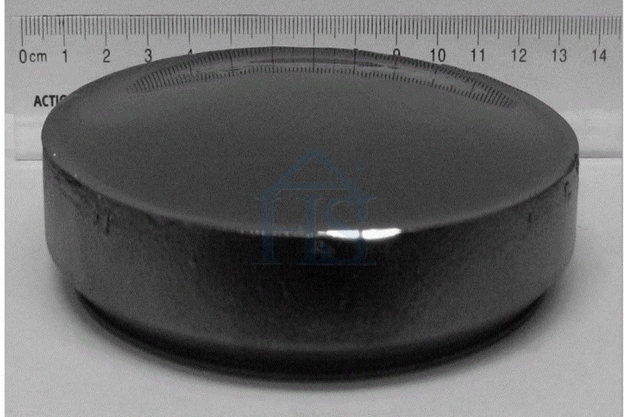
Как ведущий поставщик сырья из карбида кремния в Китае., Импорт абразивных материалов Хэнань Superior & Экспорт Ко., ООО. стабильно поставляет высокое качество черный карбид кремния а также зеленый карбид кремния для многих компаний, производящих карбид кремния по всему миру, и наши рынки охватывают США, Канада, Мексика, Перу, Чили, ОАЭ, Саудовская Аравия, Россия, Испания, Южная Африка, Юго-Восточная Азия, так далее. Если у вас есть спрос на микро порошок карбида кремния, макрозернистость карбида кремния, пожалуйста, свяжитесь с нами, чтобы получить последнее предложение карбида кремния в 2022.